"Curved CMOS Image System: When light transmitted by a lens strikes a perpendicular target such as a CMOS image sensor, it forms a circle of light called an image circle. It’s difficult for a flat (planar) CMOS image sensor to deliver high image sensitivity at high resolution (highly scaled pixel pitch) because of the fundamental physical limit known as quantum efficiency. To break through that physical limit and to achieve higher sensitivity anywhere within the image circle at higher resolution, Sony built and will describe an imaging system that comprises a hemispherically curved, back-illuminated CMOS image sensor (BIS) and integrated lens. It doubles the sensitivity at the edge of the image circle while increasing sensitivity at its center by a factor of 1.4, with a 5x reduction of dark current (Jd) compared to a planar BIS. Moreover, a common problem known as lens field curvature aberration (Afc) is mitigated by the curved sensor itself, and so the curved BIS enables higher system sensitivity with a brighter lens with a smaller F number (Fn) than is possible with a planar BIS. In addition, by controlling the tensile stress of the BIS chip to produce a curved shape in the first place, the energy band-gap (Eg) is widened and a lower Jd is achieved. (Paper T2.1, “A Novel Curved CMOS Image Sensor Integrated with Imaging System,” K. Itonaga et al., Sony)"
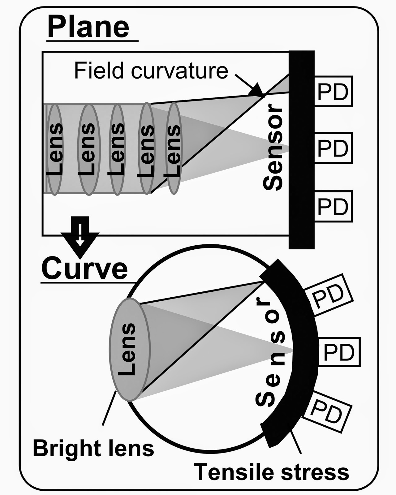 |
| Concept of an imaging system which integrates a curved sensor with a brighter (lower F number) lens for better image sensitivity. |
wondering whether this could be combined with their stacked technology...
ReplyDeleteI doubt it. The BIS (of BSI) wafer is thinned down to a few microns; it's easier to bend if it is mounted a on flexible carrier wafer (plastic??). If it is stacked on another rigid thick silicon wafer it would be difficult to do.
ReplyDeleteDo you know what was the radius of curvature of the sensor in the paper?
ReplyDeleteMakes you wonder how they dice the wafer once it is hemispherical rather than flat. The handling issues seem daunting.
ReplyDeletelooks like a human eye ball
ReplyDeleteYou should take a look at poLights polymer based piezo T-Lens. They do bend the lens in the way you commented initially
ReplyDelete